|
|||||||
|
Wafer Fab Links: See Also:
|
Wafer Fab:
Incoming Wafers
Integrated
circuits are fabricated on
single-crystal
silicon
substrates with
near-perfect
crystalline properties:
defect free and uniform crystal structure
as well as high chemical purity. These substrates are
processed in the form of
wafers,
so the fabrication of circuits on these wafers is known as
wafer
fabrication.
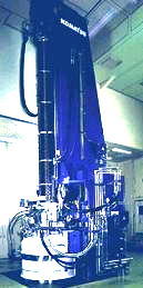
Figure 1.
Example of a Czochralski Silicon Crystal Growing Furnace
The
steps needed to obtain wafers for circuit fabrication are very
complex, but these can be simplified as follows:
1)
Quartzite,
a type of sand that's used as raw material for wafers, undergoes a
complicated
refining process to become electronic grade
polysilicon (EGS).
2)
The EGS material is then used to grow single crystal ultrapure silicon
ingots either by the
Czochralski
(CZ) or
Float Zone (FZ) method.
3) Each
ingot then undergoes
grinding,
sawing,
and
polishing
to yield many wafers.
A
wafer has to meet certain quality criteria or specifications for it to
be ready for wafer fabrication.
Electrical specifications include
the conductivity type (p or n), resistivity range, radial resistivity
gradient, and resistivity variations.
Mechanical specifications include
the diameter, thickness, total thickness variation (TTV), bow, warp,
flat dimensions, chips, indents, edge contour, bulk structural defects,
and surface orientation.
Chemical
specifications
include oxygen content, carbon content, and
oxidation-induced defects.
Surface
specifications include flatness, particle density, haze, saucer pits,
and other surface attributes.
See also: Single Crystal Growth;
Wafer Cleaning;
Wafer Specifications
1.
Ultraclean Surface Processing of Silicon Wafers: Secrets of Vlsi Manufacturing
2.
Techniques and Challenges for 300 mm Silicon: Processing, Characterization, Modelling and Equipment
3.
Crystal Growth for Beginners: Fundamentals of Nucleation, Crystal Growth, and Epitaxy
4.
Silicon Wafer Bonding Technology for Vlsi and Mems Applications (Emis Processing Series, 1)
|
||||||