|
|
|
Wafer Fab Links: See Also:
|
Wafer Fab: Ion Implantation
Ion implantation
is the
process of
depositing
a chemical species into a substrate by direct
bombardment of the substrate with
high-energy ions of the
chemical for deposition. Over the years, ion implant has steadily
replaced thermal diffusion for doping a material in wafer fabrication
because of its many advantages. The greatest advantage of ion implant
over diffusion is its more precise control for depositing dopant atoms into the substrate.
Doping, which is the primary
purpose of ion implant, is used to alter the
type
and level
of
conductivity
of semiconductor materials.
It is used to form bases, emitters, and resistors in bipolar devices, as
well as drains and sources in MOS devices. It is also used to dope
polysilicon
layers.
During ion
implantation, impurity atoms are
vaporized
and
accelerated
toward the silicon substrate. These high-energy atoms enter the
crystal lattice and lose their energy by colliding with some silicon
atoms before finally coming to rest at some depth. Adjusting the
acceleration energy controls the average depth of depositing the
impurity atoms.
Heat
treatment is used to
anneal
or repair the crystal lattice disturbances caused by the atomic
collisions.
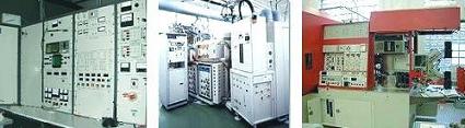
Fig.
1. Examples of Ion Implanters
As mentioned,
every implanted ion
collides
with several target atoms before it comes to a rest. Such
collisions may involve the nucleus of the target atom or one of its
electrons. The total power of a target to stop an ion, or
its total stopping power S, is the sum of the stopping power of the
nucleus and the stopping power of the electron.
Stopping
power
is described as the energy loss of the ion per unit path length of the
ion.
The
damage caused by atomic collisions during ion implantation
changes the
electrical characteristics of the target. Many target atoms are
displaced, creating deep electron and hole traps which capture mobile
carriers and increase resistivity.
Annealing is therefore
needed to repair the lattice damage and put dopant atoms in
substitutional sites where they can be electrically active again.
BOOKS on
ION IMPLANTATION
for SALE at Amazon.com:
1)
Ion Implantation: Science and Technology
2)
Handbook of Ion Implantation Technology
Copyright
©
2001-Present
www.SemiconFarEast.com.
All Rights Reserved. |