|
|||
|
MENU:
See Also:
|
What is a semiconductor? (Page 2)
<Back to Previous Page>
<Proceed to Page 3 - Field Effect
Transistors>
The Junction
Diode
A
diode is a
two-terminal electronic device consisting of a
single p-n junction. This p-n junction is usually created on a single block of silicon by doping
the block with donor and acceptor dopants at opposite ends.
A diode is a
rectifier,
allowing current to pass in one direction but not in the opposite
direction.
When
the anode (p-type side) of the diode is connected to the positive
terminal of a battery, the diode is said to be in
forward bias, allowing
current to pass through it.
The diode is said to be in
reverse bias if its cathode (n-type
side) is the one connected to the positive terminal of the battery.
A diode doesn’t conduct current in reverse bias.
A
diode only becomes forward-biased when the potential at the anode is
greater than the potential of the cathode by
0.7 V, the potential
barrier.
Under this condition, the potential barrier is effectively
'overcome' by the applied voltage, allowing the carriers of the diode to
move across the junction.
This means that the electrons from the n-type side can now go to
the p-type side in the same way that the holes in the p-type side can
now go to the n-type side.
The
current through the diode increases
exponentially as the forward-bias
voltage across the diode is increased.
Thus, the increase in the current flowing through a diode is very
abrupt once the diode starts to conduct.
In physical terms, increasing the forward-bias voltage
injects
more electrons into the n-type side of the diode. These electrons
immediately cross the junction in the absence of a potential barrier.
Once these reach the p-type material, they are pulled back to the
positive terminal of the battery again.
The holes in the p-type side also move in the same manner under
forward bias condition, although in the opposite direction as the
electrons. This continuous flow of charges through the diode will go on
as long as the diode is in forward bias.
When
a diode is put under reverse bias, the holes of the p-type side are
pulled toward the negative terminal of the battery while the electrons
in the n-type side are pulled toward the positive terminal of the
battery.
In effect, the mobile charges are pulled away from the junction
in opposite directions,
inhibiting the flow of charges through the
diode.
This is also essentially
widening
the potential barrier of the diode, making it more difficult for the
carriers to move across the junction.
In
reality, however, a very small amount of current still flows through a
reverse-biased diode.
This current, known as
reverse saturation current, is due to
thermal generation of holes and electrons near the junction of the
diode.
This is therefore dependent only on temperature and not on the
potential barrier of the diode.
The
Bipolar Transistor
The
invention of the
bipolar junction transistor in 1948 by Bardeen,
Brattain, and Shockley paved the way for the subsequent arrival of the
integrated circuit, which revolutionized the semiconductor industry.
The bipolar transistor is a
three-terminal
device consisting of 3
layers of
alternating n- and p-type materials referred to as the
emitter,
base, and
collector.
Its structure basically consists of two back-to-back diodes, one
between the emitter and base and the other between the base and
collector.
There
are two types of bipolar transistor:
the
NPN and the
PNP.
In the NPN transistor, the base is composed of a p-type material
and is sandwiched by an n-type emitter and an n-type collector.
In the PNP, the base is n-type while the emitter and collector
are p-type.
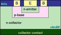
Figure 2. Structure of a planar vertical NPN bipolar
transistor
The bipolar
transistor works by yielding a
high collector current when a
relatively small current is forced into its
base.
Since Ib is relatively much smaller than Ic, a small variation in
Ib results in a much larger variation in Ic.
This, in effect, is
current
amplification,
with the current gain known as the
beta
of the transistor. The currents going into and out of
the emitter, base, and collector follow Kirchoff's current law:
Ib=Ie-Ic.
Since Ic is much greater than Ib, Ie is very close in value to Ic.
In short, a large current flows from the emitter to the collector
of a transistor whenever the base receives some input current.
The transistor is therefore very useful as a switch or as an
amplifier.
How
the transistor operates (and therefore used) depends greatly on how it
is electrically stimulated, or
biased.
The transistor may be operated in three different regions:
saturation,
cut-off, and
active.
<Back to Previous Page>
<Proceed to Page 3 - Field Effect
Transistors>
Home
Copyright
©
2001-Present
www.SemiconFarEast.com.
All Rights Reserved. |
||